5PB1102PGGI

Las imágenes son sólo para referencia
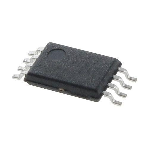
Número de pieza
5PB1102PGGI
Fabricante
Renesas / IDT
Categorías
Clock Buffer
RoHS
Ficha de datos
Descripción
Clock Buffer 1.8V to 3.3V LVCMOS 200MHz 3.465V 6VDD

Presupuesto

Fabricante
Renesas / IDT
Categorías
Clock Buffer
Maximum Input Frequency
200 MHz
Maximum Operating Temperature
+ 105 C
Minimum Operating Temperature
- 40 C
Mounting Style
SMD/SMT
Number of Outputs
2 Output
Package / Case
TSSOP-8
Propagation Delay - Max
2.9 ns
Series
5PB1102
Supply Voltage - Max
3.465 V
Supply Voltage - Min
1.71 V

últimas revisiones

Properly packed, not damaged. Works well, voltage levels are stable. Recommend.

fast delivery, item as described, thanks!!

Yes, they are all here. :)

High Quality driver, works excellent. It came to Moscow for 7 days.

The goods are OK, thank you dealers.

También te puede interesar

Gente viendo 5PB1102PGGI luego compró

Palabras clave relacionadas para 5PB1

  • 5PB1102PGGI Integrado
  • 5PB1102PGGI RoHS
  • 5PB1102PGGI Hoja de datos PDF
  • 5PB1102PGGI Ficha de datos
  • 5PB1102PGGI Parte
  • 5PB1102PGGI Comprar
  • 5PB1102PGGI Distribuidor
  • 5PB1102PGGI PDF
  • 5PB1102PGGI Componente
  • 5PB1102PGGI ICs
  • 5PB1102PGGI Descargar PDF
  • 5PB1102PGGI Descargar hoja de datos
  • 5PB1102PGGI Suministro
  • 5PB1102PGGI Proveedor
  • 5PB1102PGGI Precio
  • 5PB1102PGGI Ficha de datos
  • 5PB1102PGGI Imagen
  • 5PB1102PGGI Imagen
  • 5PB1102PGGI Inventario
  • 5PB1102PGGI Valores
  • 5PB1102PGGI Original
  • 5PB1102PGGI Mas barato
  • 5PB1102PGGI Excelente
  • 5PB1102PGGI Sin plomo
  • 5PB1102PGGI Especificación
  • 5PB1102PGGI Ofertas calientes
  • 5PB1102PGGI Precio de ruptura
  • 5PB1102PGGI Datos técnicos